College of Engineering
Semiconductor Engineering
MASTER’S
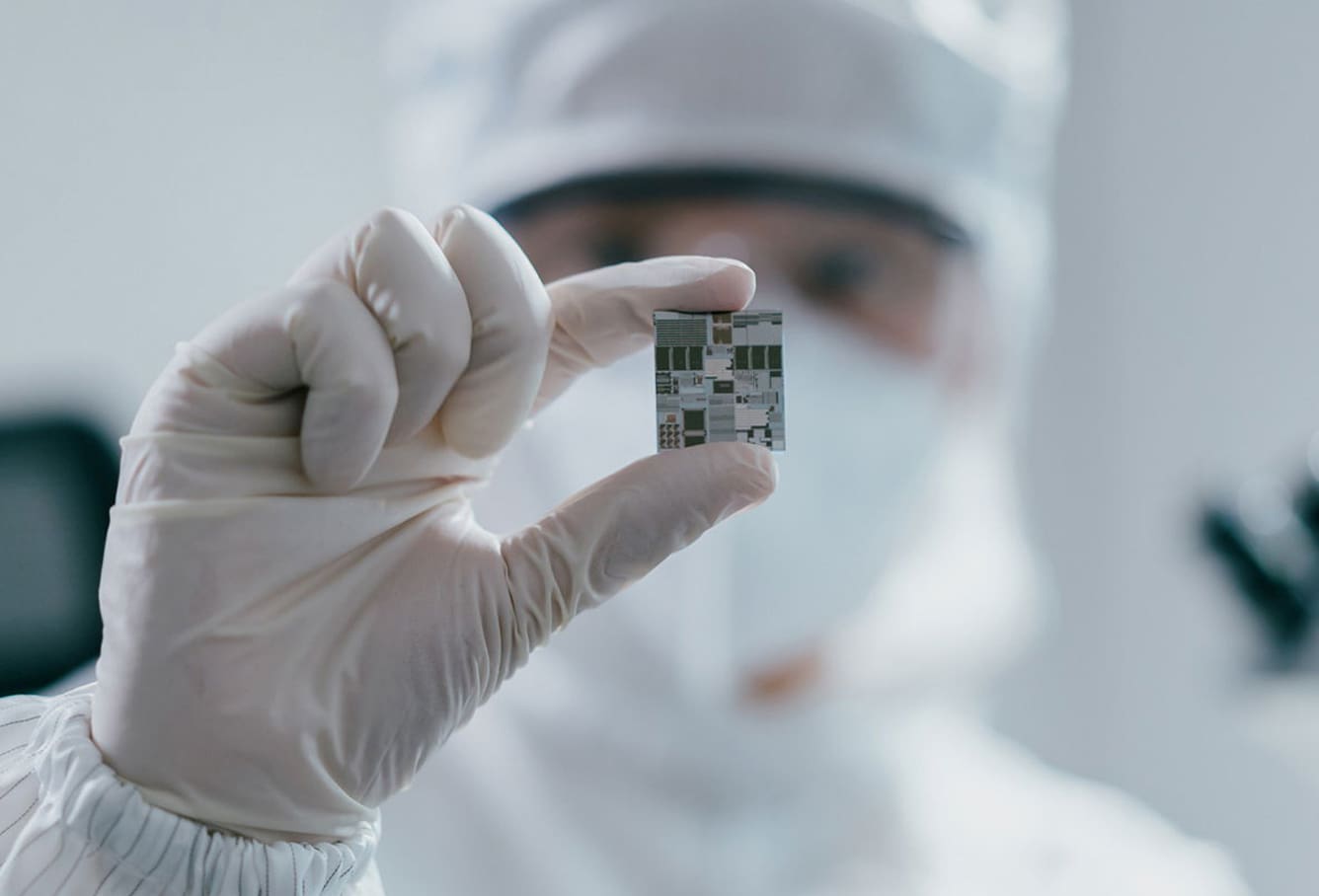
The Master of Science in semiconductor engineering will enable you to succeed in one of the world’s most vital and innovative industries. In this interdisciplinary, cutting-edge program, you’ll gain the expertise needed to address complex challenges in this rapidly evolving field.
PROGRAM FORMAT
On Ground
duration
2 – 3 Years
Meets F1 visa requirements
Yes
TIME COMMITMENT
Part time, full time
Entry term(s)
Fall
PROGRAM OVERVIEW
Create an in-demand career
This interdisciplinary, leading-edge master’s program is a collaboration among Northeastern’s College of Engineering, D’Amore-McKim School of Business, and the Institute for NanoSystems Innovation. As a student in the program, you can gain the interdisciplinary knowledge and hands-on skills to meet the urgent needs of semiconductor companies facing a talent gap.
Concentrations
Specialize in one of two industry-aligned concentrations:
- The devices and nanosystems concentration enables you to explore topics including digital and analog integrated circuit design, VLSI system design, RF and microwave circuits, power electronics, solid state devices, microelectromechanical systems (MEMS), quantum devices, optoelectronics, and silicon photonics.
- In the materials and manufacturing concentration, you’ll focus on topics such as electronic materials, semiconductor fabrication, robotics and automated manufacturing, statistical process control, statistical quality control, device reliability, additive manufacturing, and semiconductor packaging.
Unique features
- Earn your degree in the country’s first MS in Semiconductor Engineering program.
- Study in an interdisciplinary program offered through the Institute for NanoSystems Innovation, multiple departments in the College of Engineering, and the D’Amore-McKim School of Business.
- Gain research experience at an R1 research university. The program is offered through our world-leading Institute for NanoSystems Innovation in Oakland, California, one of the country’s most vibrant communities and hottest semiconductor hiring areas.
- Leverage our NanoSI entrepreneurial ecosystem, including partnerships with the largest semiconductor-based incubator programs in the country and several semiconductor-focused startups in the San Francisco Bay Area, Boston, and Burlington, Massachusetts.
- Select from three paths: thesis, project-based, or course-only options.
- Build your resumé in our top-ranked cooperative education program, allowing you to gain up to eight months of professional experience as part of your academics.
Career outlook
Earning a Master of Science in Semiconductor Engineering puts you at the forefront of a high-demand field. Since the CHIPS and Science Act in 2022, demand for skilled engineers has surged across the U.S. Additionally, the National Semiconductor Association indicates that the semiconductor industry’s workforce will grow 33% by 2030.
ADMISSIONS
Apply to the program
A graduate degree or certificate from Northeastern can accelerate your career through rigorous academic coursework and real-world professional experience in your area of interest. Apply to take your career to the next level.
Admissions dates
Applications received after the stated deadline dates will be accepted and processed as quickly as possible; however it may not be possible to have a decision rendered in time for the applicant to begin taking classes for the desired term if admitted.
Applications submitted by the referenced dates will receive full consideration for the referenced term. Applications received after the referenced dates will be considered on a case-by-case basis.
Fall Semester Entry
| Early Action: | December 1 |
| Final deadline for international students outside the U.S.: | June 1 |
| Final deadline for international students inside the U.S.: | July 1 |
| Domestic applicants: | August 1 |
Spring Semester Entry
| International students outside the U.S.: | November 1 |
| International students inside the U.S.: | December 1 |
| Domestic applicants: | December 1 |
Admissions requirements
- Completed online application form
- Application fee
- Two letters of recommendation
- Academic transcript(s) from all institutions attended
- Statement of purpose
- Resumé
- GRE is optional
- TOEFL, IELTS, or Duolingo for international applicants
PROGRAM OBJECTIVES
Prepare for success
Master the interdisciplinary knowledge and experimental tools you’ll need to fill critical roles in the rapidly evolving semiconductor industry.
Build career-advancing skills
Learn about state-of-the-art solutions relating to the semiconductor industry—from materials and manufacturing processes through device and system design, to entrepreneurship and product development.
Master the semiconductor process
Design and implement semiconductors and micro/nanosystems chips, utilizing theoretical, numerical, and experimental tools.
Keep pace with industry innovations
Anticipate and adapt to new material, structure and device requirements, system architectures, and manufacturing techniques.
COST OF ATTENDANCE
Tuition and financial aid
TUITION IN USD
$63,264
Read full tuition disclaimer
Estimated Total Tuition
This is an estimate based on the tuition rates for Academic Year 2025–2026 and does not include any fees or other expenses. Some courses and labs have tuition rates that may increase or decrease total tuition. Tuition and fees are subject to revision by the president and Board of Trustees at any time. Select programs at select campuses offer additional scholarships of up to 25% off the listed price for domestic students studying on campus. For more detailed information, please visit Student Financial Services.
For students interested in pursuing financial assistance or educational loans, additional educational costs, known as Cost of Attendance (COA) components, can be included in the calculation of aid and loan eligibility. Components may include food, housing, books, course materials, supplies, equipment, transportation, personal expenses, and the cost of obtaining a first professional licensure. You can find comprehensive details on the Student Financial Services website. Please keep in mind that COA can vary significantly depending on academic program, enrollment intensity, and individual circumstances.
There are many ways to pay for your education, including scholarships, financial aid, and more. Connect with a financial counselor to learn about your options and make your dream a reality.
Information sessions and tours
-
 Upcoming events
Sign up for virtual information sessions where you can meet Northeastern admissions staff, faculty, or even our Oakland campus dean. Find out more about our graduate programs, experiential learning in the San Francisco Bay Area, and get advice on preparing a strong admissions application.
On: Aug 04 -
Campus tours
Schedule an in-person tour and experience our beautiful Northern California campus for yourself. Meet our Oakland community, discover our world-class resources, and learn about the unique opportunities in the Bay Area’s thriving business ecosystem.
On: Jul 23


Connect with us
Want more information?
We’re here to answer your questions about this program, the application process, and more. Complete the form below to receive additional program details and speak with a member of our enrollment team.